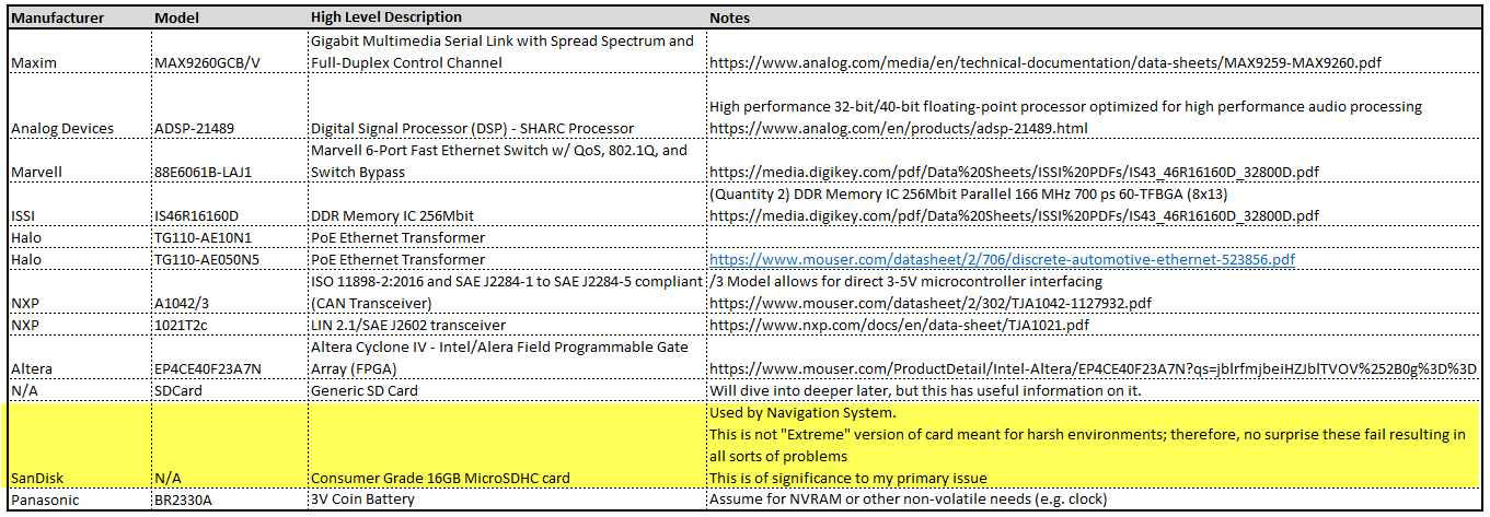
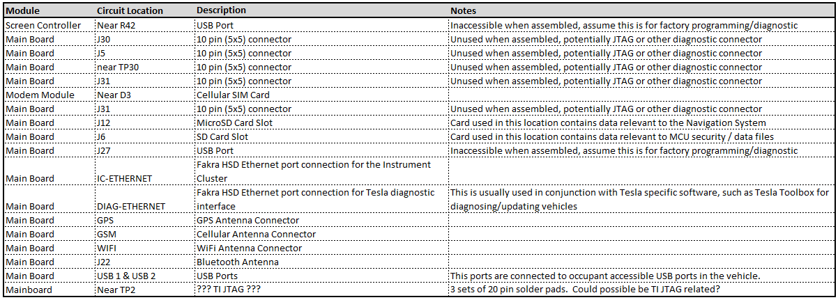
[NOTE – This post covers NLP & Sentiment Analysis at a very high level and is not intended to be an ‘all-inclusive’ deep dive in the subject. There are many nuances and details that will not be discussed in this post. Subsequent posts will dive into additional details]
NLP Overview
While modern computers can easily outperform humans in many areas, natural language processing is one area which still poses significant challenges to even the most advanced computer systems. For instance, while people are able to read Twitter posts about a given company to infer a general sentiment about the company’s performance, this type of interpretation is challenging to computers for a multitude of reasons:
- Lexical Ambiguity – A word may have more than one meaning
- I went to the bank to get a loan / I went to the bank of the river to go fishing
- Part of Speech (POS) Ambiguity – The same word can be used as a very / noun / adjective / etc. / in different sentences
- I received a small loan (noun) from the bank / Please could you loan (verb) me some money
- Syntactic ambiguity – A sentence / word sequence which could be interpreted differently.
- The company said on Tuesday it would issue its financial report
- Is the company issuing the report on Tuesday or did they talk about the report on Tuesday?
- Anaphora resolution – Confusion about how to resolve references to items in a sentence (e.g. pronoun resolution)
- Bob asked Tom to buy lunch for himself
- Does “himself” refer to Bob or Tom?
- Presupposition – Sentence which can be used to infer prior state information not explicitly disclosed
- Charles’ Tesla lowers his carbon footprint while driving
- Implies Charles used to drive internal combustion vehicles
For reasons, such as those shown above, NLP can typically be automated quite well at a “shallow” level but typically needs manual assistance for “deep” understanding. More specifically automation of Part of Speech tagging, can be very accurate. (e.g. >90%) Other activities, such as full-sentence semantic analysis, are nearly impossible to accurately achieve in a fully automated fashion.
Sentiment Analysis
One area where NLP can, and is, successfully leveraged is sentiment analysis. In this specific use case of NLP, text/audio/visual data is fed into an analysis engine to determine whether positive / negative / neutral sentiment exists for a product/service/brand/etc. While companies would historically employ directed surveys to gather this type of information, this is relatively manual, occurs infrequently, and incurs expense. As sites like Twitter / Facebook / LinkedIn provide continuous real-time streams of information, using NLP against these sources can yield relevant sentiment based information in a far more useful way.
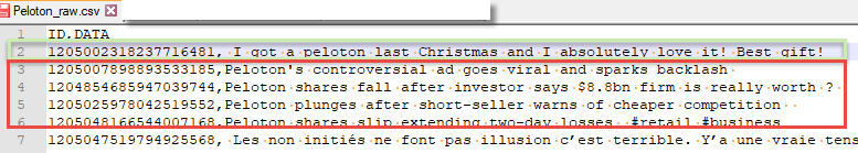
Figure 1 – Twitter Sample Data (Peloton)
In the screenshot shown above, Twitter posts have been extracted via their API for analysis on the company Peloton. A few relevant comments have been highlighted to indicate posts that might indicate positive and negative sentiment. While it is easy for people to differentiate the positive / negative posts, how do we accomplish automated analysis via NLP?
While there are numerous ways to accomplish this task, this post will provide a basic example which leverages the Natural Language Tool Kit (NLTK) and Python to perform the analysis.
The process will consist of the following key steps:
- Acquire/Create Training Data (Positive / Negative / Neutral)
- Acquire Analysis Data (from Twitter)
- Data Cleansing (Training & Analysis)
- Training Data Classification (via NLTK Naive Bayes Classifier)
- Classify Analysis (Twitter) data based on training data
- Generate Output
- Review Output / Make process adjustments / “Rinse and Repeat” prior steps to refine analysis
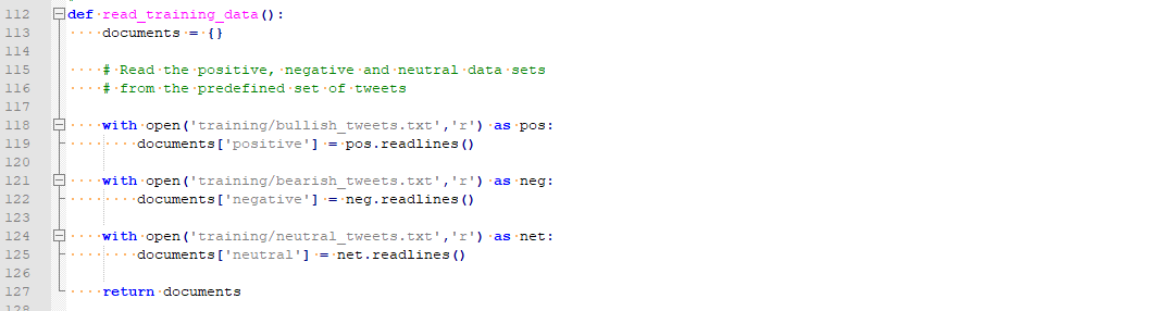
Training Data
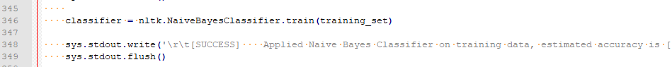
As previously discussed, it is very difficult for a computer to perform semantic analysis of natural language. One method of assisting the computer in performing this task is to provide training data which will provide hints as to what should apply to each of our classification “buckets”. With this information, the NLP classifier can make categorization decisions based on probability. In this example, we will leverage NLTK’s Naïve Bayes classifier to perform the probabilistic classifications.
As we will primarily be focused on Positive / Negative / Neutral sentiment, we need to provide three different training sets. Samples are shown below.
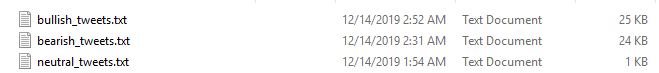
Figure 2 – Training Data
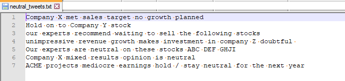
Figure 3 – Sample Neutral Training Data
NOTES:
- The accuracy of the analysis is heavily reliant on relevant training data. If the training data is of low quality, the classification process will not be accurate. (e.g. “Garbage In / Garbage Out”)
- While the examples above a pretty “easy”, not all training data is simple to determine and multiple testing iterations may be required to improve results
- Training data will most likely vary based on the specific categorization tasks even for the same source data
- Cleaning of training data is typically required (this is covered somewhat in a following section)
Acquire Analysis Data
This step will be heavily dependent on what you are analyzing and how you will process it. In our example, we are working with data source from Twitter (via API) and we will be loading it into the NLTK framework via Python. As the training data was also based on Twitter posts, we used the same process to acquire the initial data for the training data sets.
Acquiring Twitter feed data is relatively straight forward in Python courtesy of the Tweepy library. You will need to register with Twitter to receive a consumer key and access token. Additionally, you may want to configure other settings, such as how many posts to read per query, maximum number of posts, and how far back to retrieve.
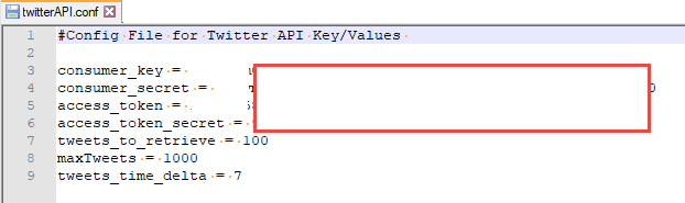
Figure 4 – Twitter API relevant variables
Once you have the correct information, you can query Twitter data with a few calls:
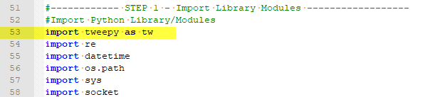
Figure 5 – Import tweepy Library
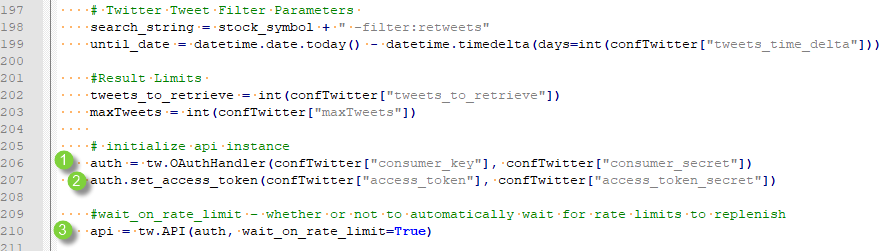
Figure 6 – Twitter Authentication

Figure 7 – Query Tweets
As NLTK can easily handle Comma Separated Value (CSV) files, the Twitter output is written out to file in this format. While Twitter returns the User ID, as well as other information related to the post, we only write the contents of the post in this example.
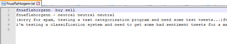
Figure 8 – Sample Twitter CSV export
Once you have a process for acquiring the training / analysis data, you will need to “clean” the data.
Data Cleansing
As you can imagine, if you start with “garbage” data, your classification program will not be very accurate. (e.g. Garbage In = Garbage Out) To minimize the impact of poor quality information, there are a variety of steps that we can take to clean up the training & analysis data:
- Country/Language specific – Remove any data that doesn’t conform with the language being analyzed. (fortunately the Twitter API provides a language filter which simplifies this)
- Remove Non-Words / Special Characters – Whitespace, Control Characters, URLs, numeric values, non-alphanumeric characters may all need to be removed from your data. This may vary depending on the exact situation; however. (e.g. Hashtags may be useful)
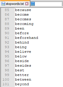
- Remove “Stop Words” – There are many words that you will find in sentences which are quite common and will not provide any useful context from an analysis perspective. As the probabilistic categorization routines will look at word frequency to help categorize the training / analysis data, it is critical that common words, such as the/he/she/and/it, are removed. The NLTK framework includes functionality for handling common stop words.Sample Stop words are shown below for reference:
- Word Stemming – In order to simplify analysis, related words are “stemmed” so that a common word is used in all instances. For example buy / buys / buying will all be converted to “buy”. Fortunately, the NLTK framework also includes functionality for accomplishing this task
- Word Length Trimming – Typically speaking, very small words, 3 characters or less, are not going to have any meaningful weight on a sentence; therefore, they can be eliminated.
Once the data has been cleansed, training categorization can occur.
Training Data Categorization
As referenced previously, the sentiment analysis is performed by providing the NLP process training data for each of the desired categories. After stripping away the stop words and other unnecessary information, each training data set should contain word / word groupings which are distinct enough from each other that the categorization algorithm (Naïve Bayes) will be able to best match each data row to one of the desired categories.
In the example provided, the process is essentially implementing a unigram based “bag of words” approach where each training data set is boiled down into an array of key words which represent each category. As there are many details to this process, I will not dive into a deeper explanation in this post; however, the general idea is that we will use the “bag of words” to calculate probabilities to fit the incoming analysis data.
For example:
- Training Data “Bag of Words”
- Positive: “buy”, “value”, “high”, “bull”, “awesome”, “undervalued”, “soared”
- Negative: “sell”, “poor”, “depressed”, “overvalued”, “drop”
- Neutral: “mediocre”, “hold”, “modest”
- Twitter Analysis Sample Data (Tesla & Peloton)
- Tesla : “Tesla stock is soaring after CyberTruck release” = Positive
- Peloton: “Peloton shares have dropped after commercial backlash” = Negative


The unigram “bag of words” approach described above can run into issues, especially when the same word may be used in different contexts in different training data sets. Consider the following examples:
- Positive Training – Shares are at their highest point and will go higher
- Negative/Neutral Training – Shares will not go higher, they are at their highest point
As the unigram (one) word approach looks at words individually, this approach will not be able to accurately differentiate the positive/negative use of “high”. (There are further approaches to refine the process, but we’ll save that for another post!)
IMPORTANT – The output of this process must be reviewed to ensure that the model works as expected. It is highly likely that many iterations of tweaking training data / algorithm tuning parameters will be required to improve the accuracy of your process.
Analysis Data Categorization
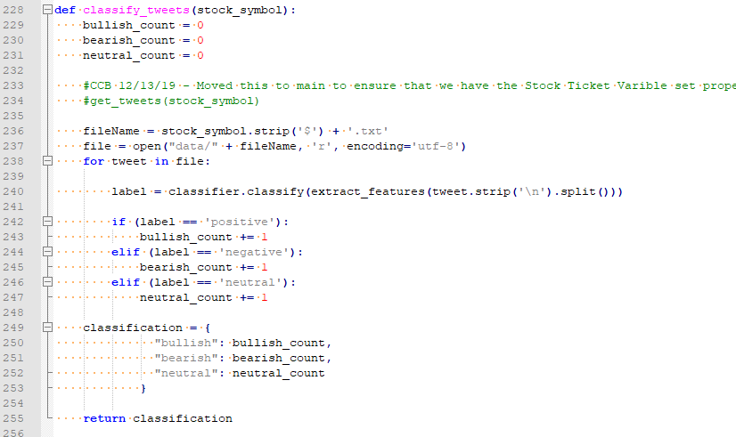
Once the training data has been processed and the estimated accuracy is acceptable, you can use iterate through the analysis data to create your sentiment analysis. In our example, we step through each Twitter post and attempt to determine if the post was Positive / Negative / Neutral. Depending on the classification of the post, the corresponding counter is incremented. After all posts have been processed, the category with the highest total is our sentiment indicator.


Generate Analysis
Once all of the pieces are in-place, you can run your process and review the output to validate your model. To simplify the testing, I created a fictitious phrase [FnuaFlaHorgenn] and created a handful of Twitter posts referencing it. I then ran the program to verify that it correctly classified the Twitter post(s)

Figure 9 – Sample Twitter Post

Figure 10 – Twitter API Extract
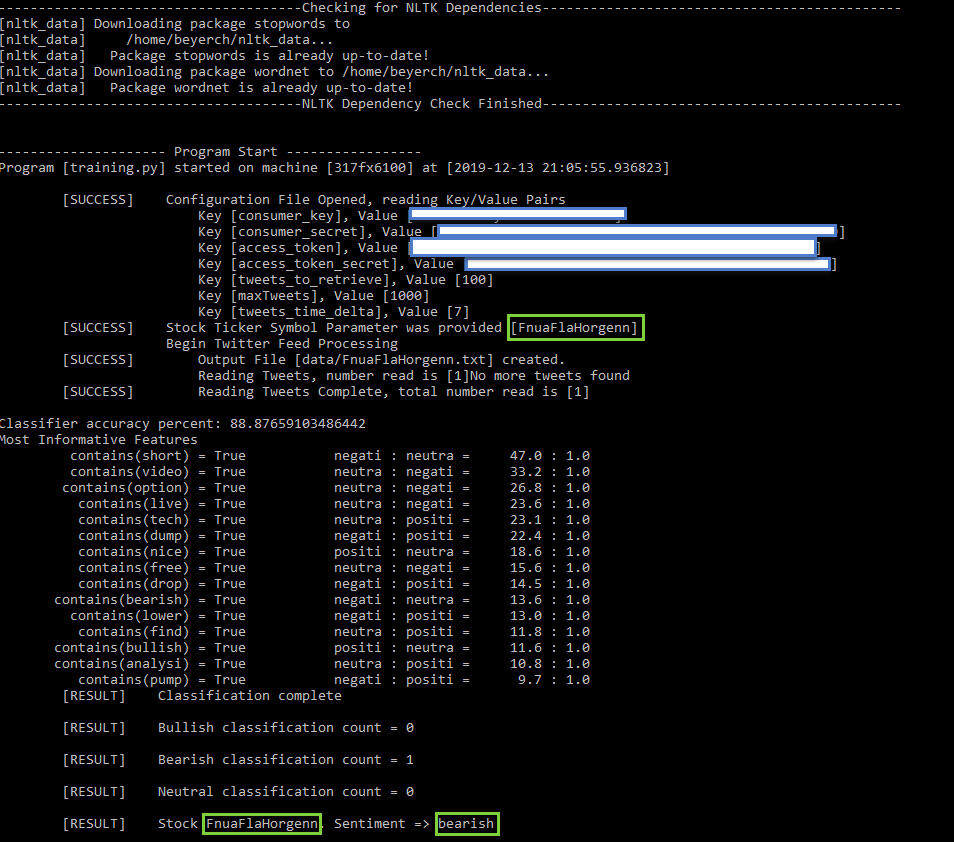
Figure 11 – Program Output (Bearish)
Conclusion
While NLP is not perfect and has limits, there are a wide variety of use cases where it can be applied with success. The availability of frameworks, such as NLTK, make implementation relatively easy; however, great care must be taken to ensure that you get meaningful results.
 Overview